| High Voltage Electron Microscopy (HVEM) |
| High Voltage Electron Microscopy (HVEM) |
calculated by the McKinley-Feshbach formula Table 1 Threshold energy (Ed), threshold acceleration voltage (Ud), and cross section (s) for atomic displacement of pure element by fast electron irradiation [1, 2]. Most of the values for Ed and Ud were taken from the references [3-5]. A list of the systematic experimental data was firstly summarized by K. Urban [3,4] and slightly modified by H. Fujita [5]. The s values were calculated using the McKinley-Feshbach formula, which is frequently used in radiation damage analysis [6-9]. (Updated on 02/21/2014) 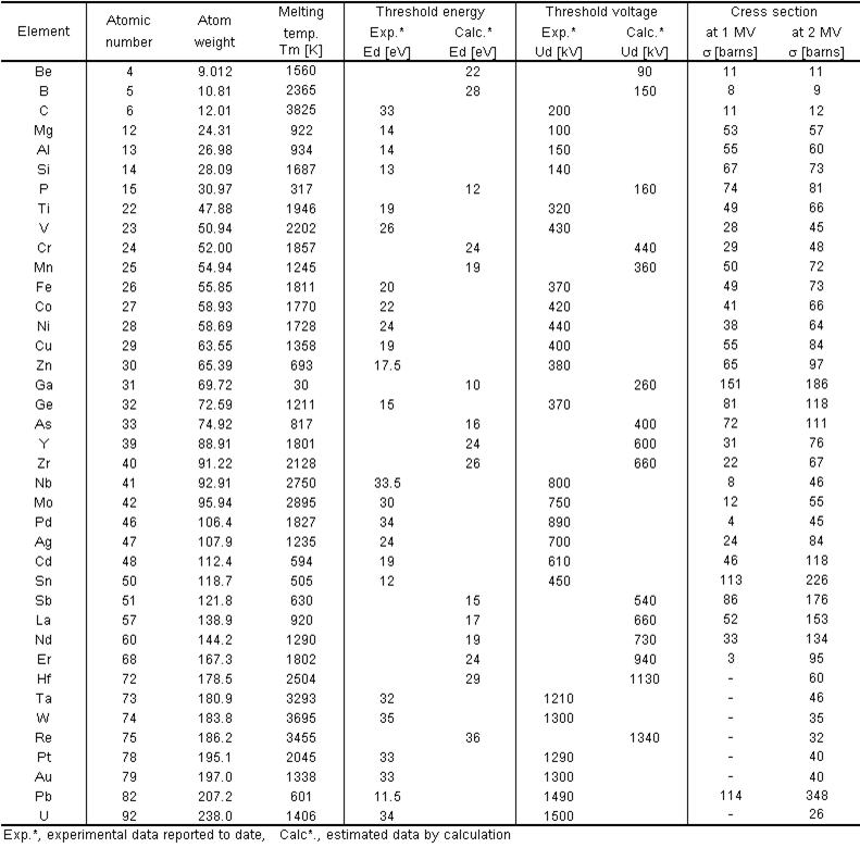 Figure 1 Cross section (s) for atomic displacement of pure element by fast electron irradiation. Most of the values for Ed and Ud were taken from the references [3-5]. The s values were calculated using the McKinley-Feshbach formula, which is frequently used in radiation damage analysis [6-9]. (Updated on 02/20/2014) 012 Mg (Atomic number 12, Atomic mass number 24.31, Ed 14 eV) 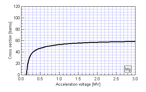 013 Al (Atomic number 13, Atomic mass number 26.98, Ed 14 eV) 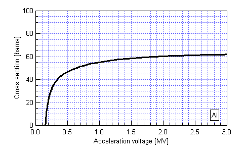 014 Si (Atomic number 14, Atomic mass number 28.09, Ed 19 or 13 eV) 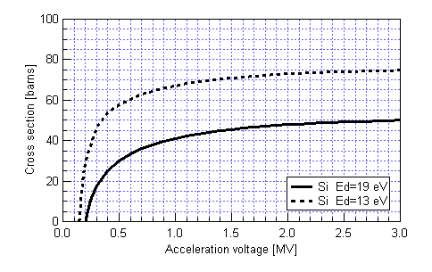 022 Ti (Atomic number 22, Atomic mass number 47.88, Ed 19 eV) 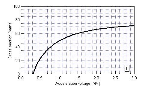 023 V (Atomic number 23, Atomic mass number 50.94, Ed 26 eV) 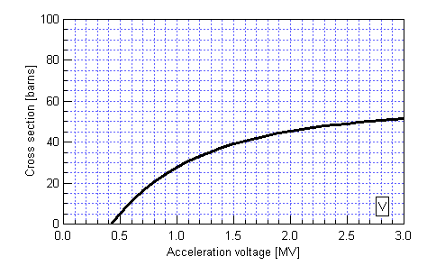 024 Cr (Atomic number 24, Atomic mass number 51.9961, Ed 26 eV) 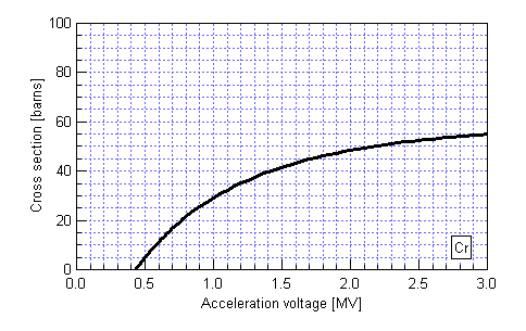 026 Fe (Atomic number 26, Atomic mass number 58.93, Ed 22 eV) 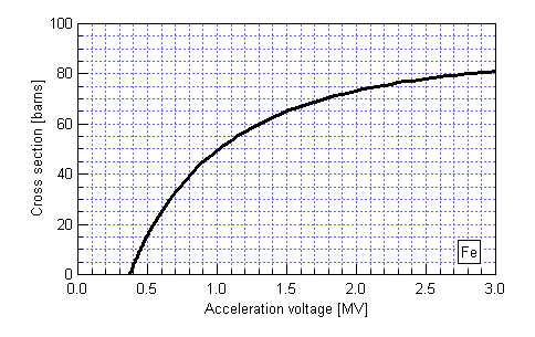 027 Co (Atomic number 27, Atomic mass number 58.93, Ed 22 eV) 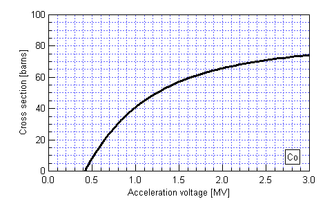 028 Ni (Atomic number 28, Atomic mass number 58.69, Ed 24 eV) 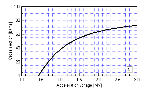 029 Cu (Atomic number 29, Atomic mass number 63.55, Ed 19 eV) 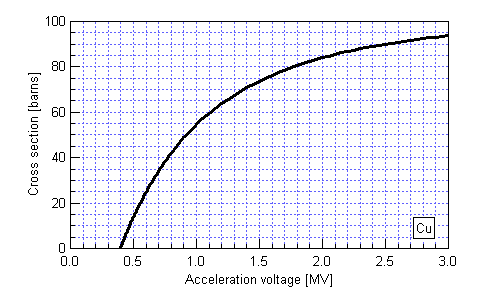 040 Zr (Atomic number 40, Atomic mass number 91.22, Ed 26 eV) 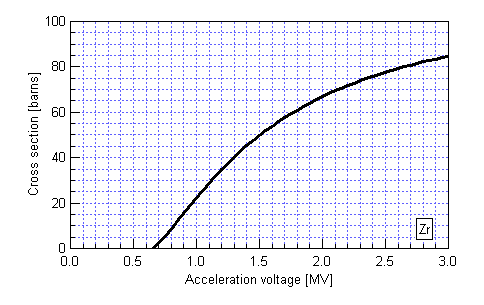 041 Nb (Atomic number 41, Atomic mass number 92.21, Ed 33.5 eV) 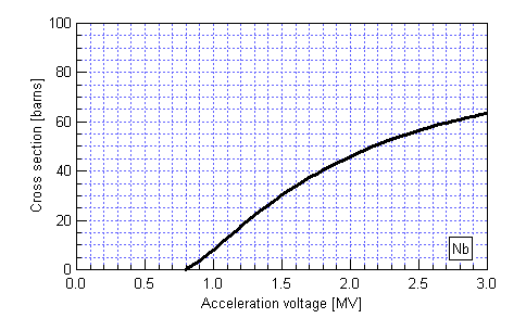 042 Mo (Atomic number 42, Atomic mass number 95.94, Ed 30 eV) 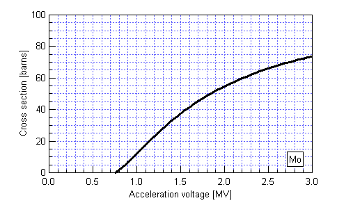 046 Pd (Atomic number 46, Atomic mass number 106.4, Ed 34 eV) 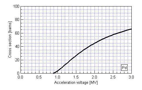 047 Ag (Atomic number 47, Atomic mass number 107.9, Ed 24 eV) 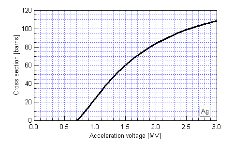 050 Sn (Atomic number 50, Atomic mass number 118.7, Ed 12 eV) 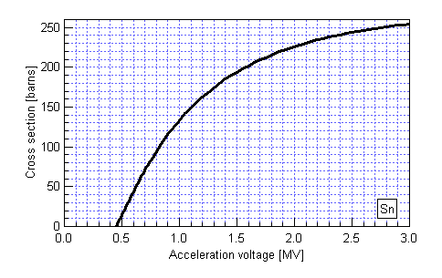 051 Sb (Atomic number 51, Atomic mass number 121.75, Ed 14.6 eV) 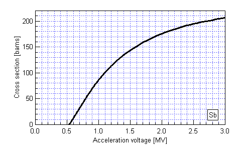 060 Nd (Atomic number 60, Atomic mass number 144.2, Ed 19 eV) 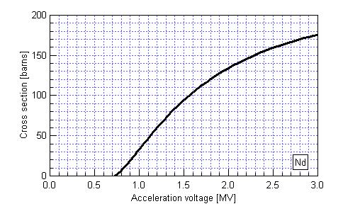 072 Hf (Atomic number 72, Atomic mass number 178.5, Ed 29 eV)  073 Ta (Atomic number 73, Atomic mass number 180.9, Ed 32 eV) 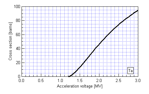 074 W (Atomic number 74, Atomic mass number 183.84, Ed 35 eV) 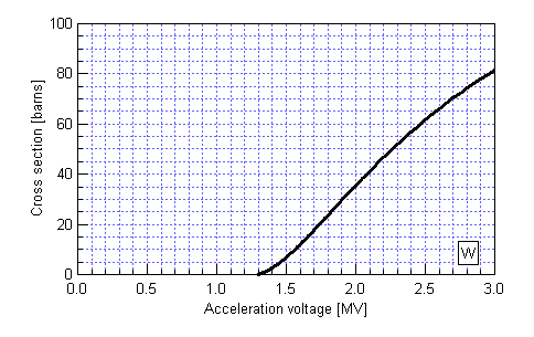 078 Pt (Atomic number 78, Atomic mass number 195.1, Ed 33 eV) 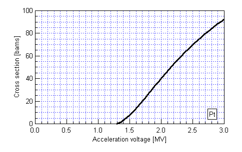 079 Au (Atomic number 79, Atomic mass number 197, Ed 33 eV)  REFERENCE [1] T. Nagase (Contribution): Advanced materials design by irradiation of high energy particles, in: Progress in Advanced Structural and Functional Materials Design, Ed., T. Kakeshita, Springer, 2013. pp. 137-153. ISBN 978-4-431-54063-2 http://www.springer.com/materials/structural+materials/book/978-4-431-54063-2 [2] T. Nagase, T. Sanda, A. Nino, W. Qin, H. Yasuda, H. Mori, Y. Umakoshi, and J.A. Szpunar: J. of Non-Cryst. Solids, 358, 502-518 (2012). http://dx.doi.org/10.1016/j.jnoncrysol.2011.11.010 [3] K. Urban: Phys. Stat. Sol. A 56, 157–168 (1979) [4] K. Urban: Electron Microsc. 4, 188–195 (1980) [5] H. Fujita: Hiheikou-zairyo no Riron to Gijyutsu, Seminar text of Japan Institute of Metals, 73–82 (1989) (in Japanese) [6] W.A. Mckinley, H. Feshbach: Phys Rev., 74, 1759-1763 (1948). [7] F. Seitz, J.S. Koehler: in: Seitz, F., Tumbull, D. (Eds.) Solid State Physics, Vol. 2, Aca-demic Press, New York, (1956) [8] J.W. Corbett: in Electron Radiation Damage in Semiconductors and Metals, Academic Press, New York, (1966) [9] O.S. Oen: Nucl. Instrum. Methods Phys. Res. Sect. B 33, 744–747 (1988). |
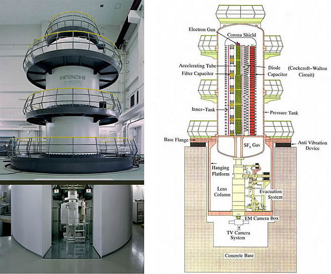 Figure 1 Ultra-High Voltage Electron Microscope - Hitachi H-3000 in Osaka University The 3 MV ultra-high voltage electron microscope (Hitachi H-3000) was developed based on various advanced technologies, such as the high stability of the high voltage generating circuit, the reduction of power losses, the improvement of the response speed of the objective lens, negative ion removal equipment, a remote control system, and an online image enhancement system. The ultra-high voltage electron microscope is widely used by researchers in many fields, including materials science, nanotechnology, biology, and medical science. The particular advantages of the H-3000 can be summarized as follows: 1. Remarkable increases in the maximum observable thickness of a specimen. 2. Various types of in-situ observations made possible by the very large specimen space. 3. Lattice defect introduction and/or non-equilibrium phase formation through the interaction between high energy electrons and constituent elements in materials. Main specifications High voltage generator Symmetrical Cockcroft–Walton circuit: 35-stage Electricity consumption in high voltage tank: under 1 kW Acceleration voltage: Normal: 3.0 MV (3000 kV) Medium: 0.5, 1.0, 1.5, 2.0, 2.5 MV Maximum: 3.5 MV Stability of high voltage: less than 2.0×10⁻⁶/min Electron gun and acceleration tube Cathode: LaB6 single crystal (thermal type) Beam current: maximum 20 mA Acceleration tube: 22 kV/step × 138 steps (3 MV) Insulating gas: SF6 (4 atom) Irradiation lens system Ion trapping system: electron beam shift by polarization coil Lens constitution: double-condenser lens Beam angle: less than 10-3 Imaging lens system Lens configuration: six-step lens system (no image rotation) Magnification: 200 to 1,000,000 (30-step switching) Camera length at electron diffraction: maximum 14 m (six-step switching) Resolution: less than 10 nm Objective lens Magnetomotive force: maximum 23 A/V1/2 (3 MV) Focusing length: less than 11 mm Spherical aberration coefficient: less than 10 mm Chromatic aberration coefficient: less than 10 nm Defocused point: minimum 5 nm Specimen space Holder: Top-entry type and side-entry type Orientation angle of top-entry type: ±30 degrees (double-tile type) Orientation angle of side-entry type: ±45 degrees (double-tile type) Specimen motion: ±1 mm (mechanical system), ±1.5 mm (electrical system) Vacuum: 5×10⁻⁶ Pa (oil-free vacuum system) Camera room and operation room Photo system: imaging plate (32 sheets × 2), film (50 sheets × 2) Fluorescent substance: P22, YAG Fluorescent screen: maximum 60 × 80 mm TV camera High resolution type: 1125-line HARP camera High sensitivity type: slow-scan CCD camera with cooling Video recording: NTSC mode HARP camera Remote control system Operation system: Console panel for remote operation Controlling system: main control workstation system and decentralized data processing system Monitoring system: X-ray, oxygen deficiency, beam position, specimen holder |
Review papers about Materials Science based on High Voltage Electron Microscopy are the followings. REFERENCE [1] H. Fujita: J. of Electron Micro. Tech. 3, 243–304 (1986) [2] H. Fujita.: J. of Electron Micro. Tech. 12, 201–218 (1989) [3] A. Seeger: J. of Electron Micro. 48, 301-305 (1999) [4] H. Fujita: Proc. Jpn. Acad., Ser. B, Vol. 81, 141-155 (2005) . [5] H. Mori: J. of Electron Micro., 60, S189-S197 (2001) [6] H. Yasuda: Kenbikyo, 46, 160-164 (2011) (in Japanese) |